Table of Contents
Accessing S88 feedback bus from Ethernet
Preface
The S88 bus is a feedback bus system for model railroad systems.
Up to 32 decentralized slaves connected to each other in a serial fashion controlled by one master device (control unit). The slaves are spreaded around model railroad layout. Each slave has parallel connected IOs which are loaded via an master activated LOAD control line into a local parallel register of typical 8 bits width. Now all slaves build up virtual one shift register and the master shifts in each bit from the bus with CLOCK signal. The control unit can further process the received data afterwards. Often a third control signal RESET is used to bring the bus into a well known state.
The S88 bus therefore consists of 3 control lines, CLOCK, LOAD und RESET and one data line, DATA.
More details about S88 bus: S88N standard.
Netzer as computing unit
Because of its flexibility it is very easy to read out an S88 section with Netzer. The serial server in SPI master mode is used for that. Among using the bus itself the possibility of controlling IO pins with escape sequences is used here.
Hardware
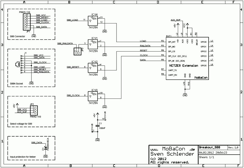
The picture shows a circuit for the Netzer Playground S88 Extension board. The used parts are standard components, which can be build up fast also on a grid-style board.
The circuit is simple and explained very quickly. Netzers operation voltage is +3.3V. The voltage level of the S88 bus is usually +5V. Therefore an interface is used for the three control lines RESET, LOAD and CLOCK - a simple 74 bus driver with tristate output (IC1). The tristate is not used here, the enable pin is tied to ground. C1 is the blocking capacitor for IC1.. +5V is supplied by Netzer Playground.
J1 offers an old-style S88 connection. JP1 is a RJ45 socket for the new wiring standard S88N.
The wiring standard S88N also permits +12V (all modules on the bus must support it!!!) as alternative supply voltage to the +5V. For switching the power supply JP2 must be jumpered accordingly. VCC_AUX is the primary supply voltage from Netzer Playground and should be adjusted to +12V if used.
Pin 8 of the S88N standard is for the rail control signal (like DCC). For testing purposes the SPI output also is interfaced through the bus driver - maybe for later controlling applications (if JP3 is jumpered).
The returning bus data line DATA is connected directly to Netzer. This is possible because the SPI input is +5V tolerant. The suppressor diode D1 is an additional protection against spikes from the bus.
The further documentation assumes that LOAD is connected to SPI_INT and RESET is connected to SPI_CS.
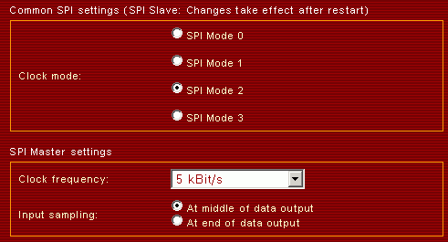
Settings Netzer web interface
Netzer with installed IO firmware (at least Release *1.5pro*) must be configured via the webinterface:
- SPI-Master-Mode on the common page (restarting Netzer afterwards is needed)
- SPI-Master settings: Frequency on 5 kHz (for long lines also 1.3 kHz may be tried), SPI mode 2 (Idle state of the clock signal is 1, data is stored on falling edge), sampling of the data in the middle of clock cycle (see picture)
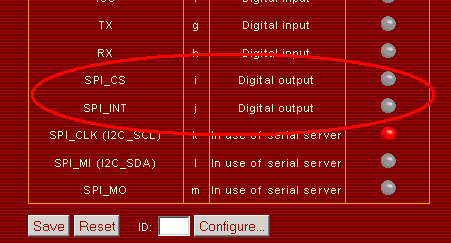
- GPIO settings: In this example SPI_INT and SPI_CS are use as digital outputs. Configure them via the GPIO settings dialog!
Connection establishment
For a simple connection test use a terminal program which is able to send and receive bytes in hexadecimal or binary representation like the Hammer-Terminal). The Netzer Connections itself can established from PC with i.e. com2tcp. On Linux systems simply use netcat.
Example protocol
For the generation of the correct control sequence use the following:
| # | ASCII representation | Hexadecimal representation | Explanation |
|---|---|---|---|
| 1 | \1 | 0x5C 0x31 | Switch over the SPI mode to mode 1. CLOCK automatically changes from 1 to 0. |
| 2 | \J | 0x5C 0x4A | LOAD (at INT-Pin) is set. |
| 3 | \t | 0x5C 0x74 | Wait minimum 100 µs (silence). |
| 4 | \2 | 0x5C 0x32 | Reset SPI mode to mode 2. CLOCK automatically changes from 0 to 1. At this point the IOs are loaded into the register through the active LOAD signal. |
| 5 | \I | 0x5C 0x49 | Activating RESET (at CS-Pin) from 0 to 1. Reset the bus devices to well known state. |
| 6 | \i | 0x5C 0x69 | Reset RESET from 1 to 0. |
| 7 | \j | 0x5C 0x74 | Reset LOAD from 1 to 0. Now the bus is prepared for shifting in all the data. |
| 8… | a | 0x61 | Now unlimited data can be shifted in (but should limited up to 32 or the number of connected slaves). Each sent random byte (without escape sequence) shifts 8 bits in (normal SPI mode). After reception the data is sent via socket to the PC application. |
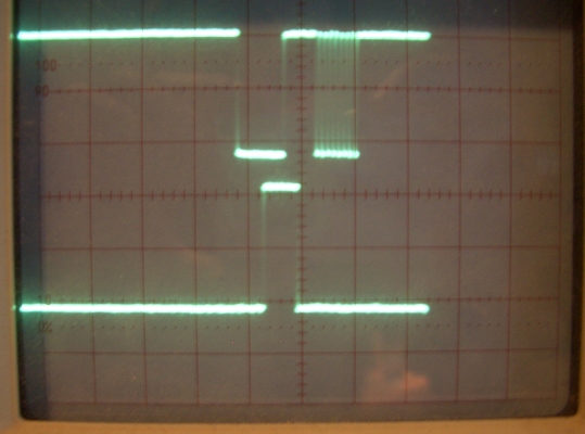
And here is a live picture from test circuit (the upper curve is clock, the lower is LOAD - timing of the first shifted byte):
PC application
Coming soon…


